A KU Research Group Develops Precision Quantum Dot Patterning Technology to Enable Ultra-High-Resolution AR/VR Displays
- categorization Research
- writing date 2025.10.17
- author Communication Team
- hits 112
A KU Research Group Develops Precision Quantum Dot Patterning Technology to Enable Ultra-High-Resolution AR/VR Displays
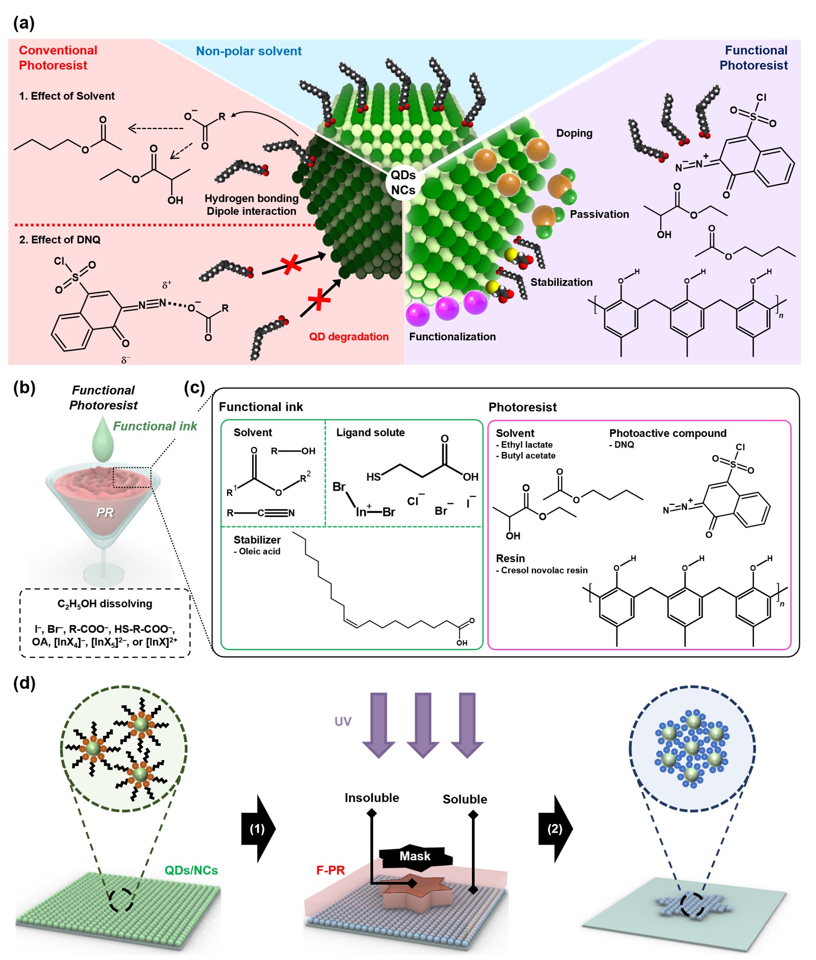
△ A schematic illustration of a functional photoresist (F-PR) applicable to quantum dots (QDs)/nanocrystals (NCs) and a process diagram of QD/NC patterning
Professor Oh Soong-joo’s group in the Department of Materials Science and Engineering at KU (President: Kim Dong-One) has developed a novel patterning technology capable of precisely processing quantum dots (QDs) and nanocrystals (NCs), thereby enabling semiconductor fabrication processes for the achievement of miniaturization and the enhanced performance of electronic and optoelectronic devices.
*Quantum dots (QDs): Tiny semiconductors measuring only several nanometers (nm), whose electrical and optical properties change depending on their size.
*Nanocrystals (NCs): Particles with at least one dimension less than 100 nanometers (nm), or one ten-millionth of a meter.
*Patterning: A miniaturization process that uses light or chemical reactions to engrave a desired shape on the material surface of a material.
The results of this study were published online on August 26 in Materials Today (IF=22.0), a globally renowned journal.
*Article title : Surface chemistry stabilized photolithography for high-resolution quantum dot electronic and optoelectronic devices
*DOI: 10.1016/j.mattod.2025.08.018
*URL: https://doi.org/10.1016/j.mattod.2025.08.018
Despite their small size, QDs emit vivid light and exhibit excellent electrical properties, making them a promising material for next-generation displays, image sensors, wearable devices, and biosensors. However, their extremely small size makes it difficult to utilize them in actual devices, as their surfaces are easily damaged or their properties are altered in conventional semiconductor manufacturing processes.
To address this issue, the research group developed a new “QD surface-stabilized functional photoresist (F-PR).” F-PR is made by combining a photosensitive compound, a stabilizer, and a surface-protecting ligand, and it can overcome the limitations of existing photoresists and stably maintain the properties of QDs. Using this material, the research group successfully formed precise patterns without compromising the inherent properties of QDs.
*Photoresist: A material that hardens or melts in response to light and is used to engrave circuit patterns on a semiconductor surface.
In particular, the research group applied this technology to the reduction of pixel sizes to less than 6 μm (micrometers) and to achieve an ultra-high resolution of up to 4,200 pixels per inch (PPI). This enabled successful production of various high-performance devices, which may be achieved using the general semiconductor processing equipment, making them advantageous for large-scale industrial applications.
Professor Oh said, “Our study has made it possible to produce high-resolution photoresist-based QD devices, which was previously thought to be impossible. Our results will accelerate the commercialization of ultra-high-resolution, high-performance products in various fields such as AR/VR displays, healthcare sensors, and next-generation optoelectronic devices.”
This study was supported by the Ministry of Science and ICT and the National Research Foundation of Korea.
[Figure]